The KD2BD 9600 Baud Modem
By: John A. Magliacane, KD2BD
|
The KD2BD 9600 Baud Modem
By: John A. Magliacane, KD2BD |
|
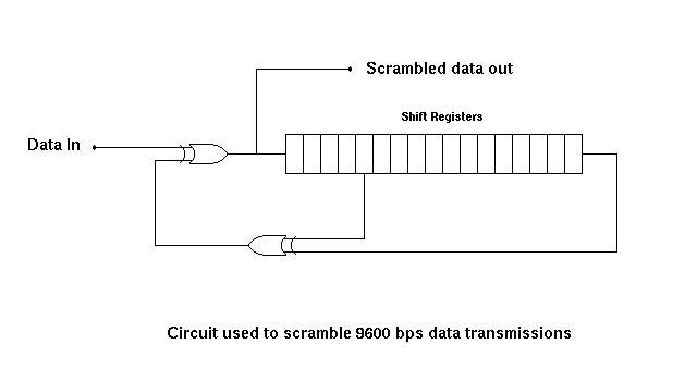
Figure 1: Block diagram illustrating the scrambler circuitry used in 9600 baud amateur communications. This particular design is based on the use of shift registers and exclusive-OR gates.
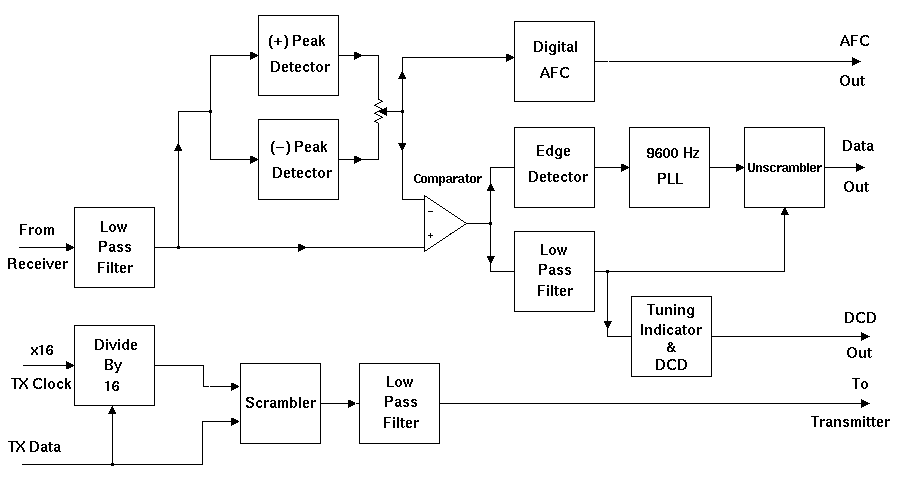
Figure 2: Block diagram of the KD2BD 9600 Baud Modem. Both receive and transmit sections function independently of one another allowing full-duplex communications with pacsat satellites.
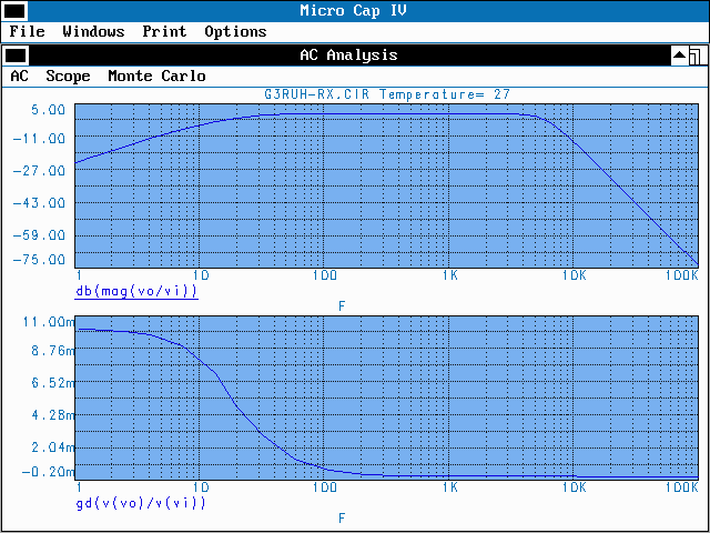
Figure 3: Simulated performance of the receive filter used in the G3RUH 9600 Baud Modem. In this figure, voltage gain and group delay characteristics are both plotted as a function of frequency. This filter exhibits uneven frequency response and excessive group delay distortion below 40 Hz.
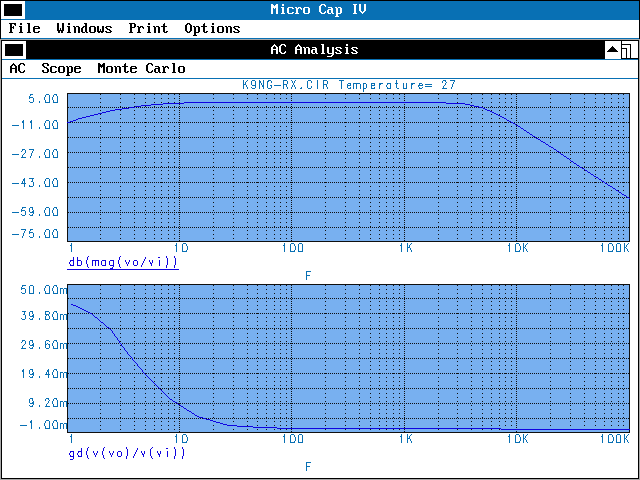
Figure 4: Simulated performance of the receive filter used in the K9NG/TAPR 9600 baud modem. In this figure, voltage gain and group delay characteristics are both plotted as a function of frequency. While better than the G3RUH filter, the K9NG/TAPR filter simulation shows low frequency roll-off and group delay distortion.
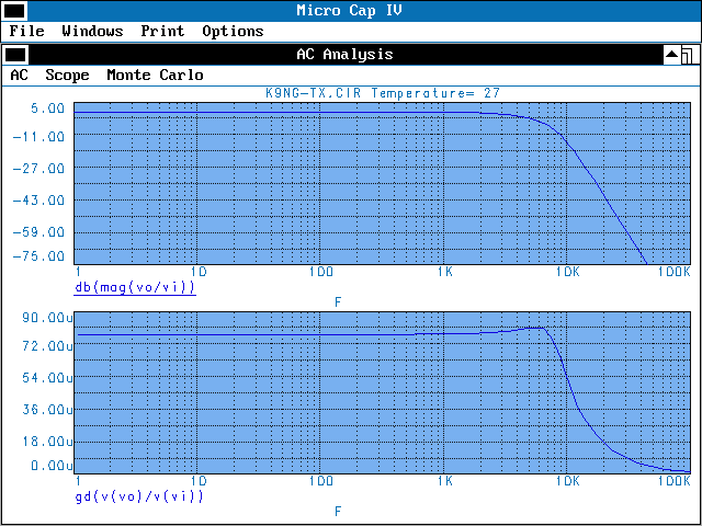
Figure 5: Simulated performance of the transmit filter used in the K9NG/TAPR 9600 baud modem. This graph plots voltage gain and group delay characteristics as a function of frequency.
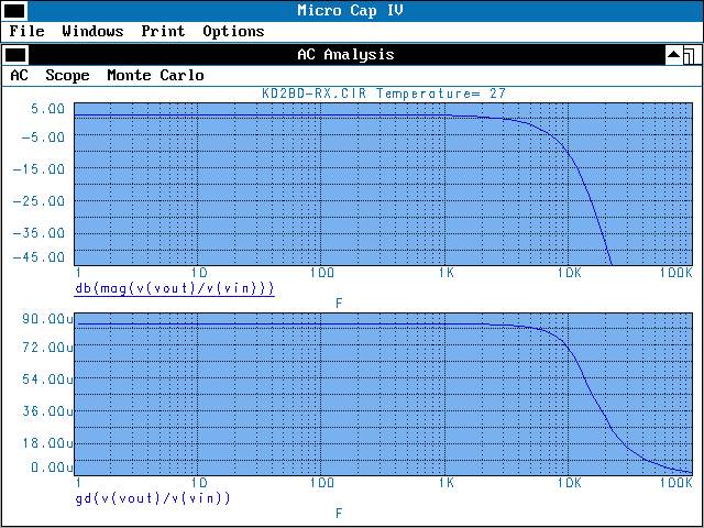
Figure 6: Simulated performance of the receive filter used in the KD2BD 9600 Baud Modem. This graph plots voltage gain and group delay as a function of frequency. Notice that both plots show exceptionally flat response across the entire frequency range of operation, providing superb demodulator performance.

Figure 7: Simulated performance of the transmit waveform shaping filter used in the KD2BD 9600 Baud Modem. This graph plots voltage gain and group delay as a function of frequency. Notice that both plots show exceptionally flat response across the entire frequency range of operation, providing superb modulator performance.
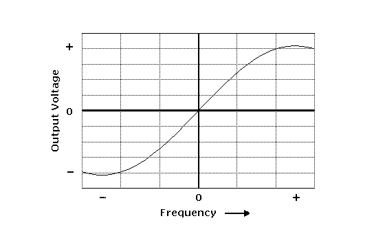
Figure 8: Response characteristics of a linear FM demodulator are plotted as a function of frequency. Quadrature detectors have similar characteristics except the center of their response is elevated such that their output voltage is always positive.
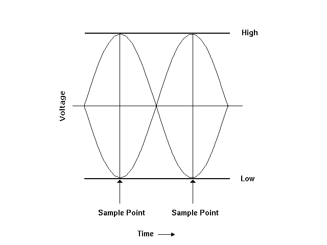
Figure 9: A plot of several filtered bits over time yields an "eye diagram" pattern. Sampling the "eye" at its center provides proper signal detection with the highest signal-to-noise ratio possible.
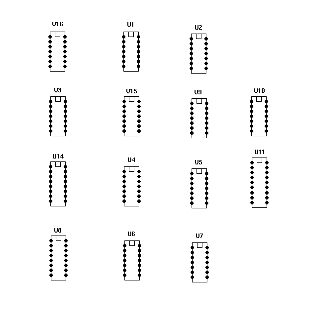
Figure 10: Parts placement of DIP ICs used in the KD2BD 9600 Baud Modem.
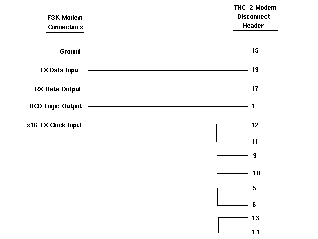
Figure 11: Connections between the KD2BD 9600 Baud Modem and a TAPR TNC-2 or clone are made at the TNC's modem disconnect header. Consult your TNC manual to determine connections for other TNCs.
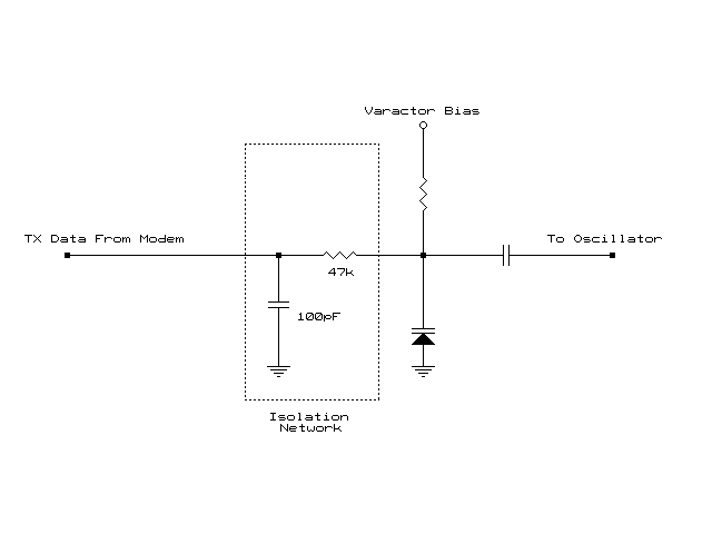
Figure 12: A simple RC isolation network is required to connect the FSK Output of the KD2BD 9600 Baud Modem to the varactor of an FM voice transmitter to generate an FSK signal at RF frequencies.
 Return to the KD2BD 9600 Baud Modem Page