Chuck Green, Peter Gülzow
Lyle Johnson, Karl Meinzer, James Miller
As so often happens, these seemingly unrelated events were the mutual catalysts that led to a small group of us discussing, designing, building and debugging a major new spacecraft computer for inclusion on P3D!
Immediately after the P3D IHU was brought to life in 1995, the I/O multiplexer was designed. While various proposals had been made, none seemed acceptable to reliably replace the parallel wiring that controls the various modules on P3D and provides status. The wiring bundles in P3D are extensive, massive and complex. More than 200 wires fan out from the multiplexer to destinations all over the spacecraft.
The CAN bus implemented on P3D offers some promise of relieving wiring complexity. In fact, many experiments on P3D are tied together by the CAN bus, and some of them rely solely on it. But the CAN protocols require a processor and the simplest systems continuously draw over 100 mW of spacecraft power. However, this situation is improving with the growing popularity of the CAN standard.
Current rad-hard processors are extremely expensive, or use a lot of power, or both.
An eerily AMSAT-like sequence of events in the mid 1980s led to the development of the Acorn RISC Machine (ARM). This was a 32-bit RISC processor developed by a team of four people at Acorn Computers, Ltd. [1] [10.1]. Acorn at the time was the leading UK manufacturer of small computers for education and home use. Goals of the processor design included simplicity, low-power operation, and moderate performance at low cost. First silicon appeared in 1985 and the first desktop computer using the ARM-2 in 1987.
In 1990, Apple, Acorn and VLSI Technology co-founded Advanced RISC Machines to exploit the ARM architecture. This was to be a fabless company, and was an early embodiment of the now-popular intellectual property (IP) semiconductor business paradigm.
The ARM processor has evolved over the ensuing years. In 1994, Digital Semiconductor licensed the ARM technology with an agreement to dramatically increase its performance. It resulted in the StrongARM processor in 1996, which Acorn themselves immediately incorporated into their flagship product, the Acorn RISC PC.
The StrongARM is a 32-bit RISC processor with on-chip instruction and data cache, a memory management unit (MMU), and the ability to deliver over 200 MIPS sustained performance while consuming about 0.5 watt. This compares to, for example, a "mobile Pentium" which delivers similar performance but uses nearly 8 watts.
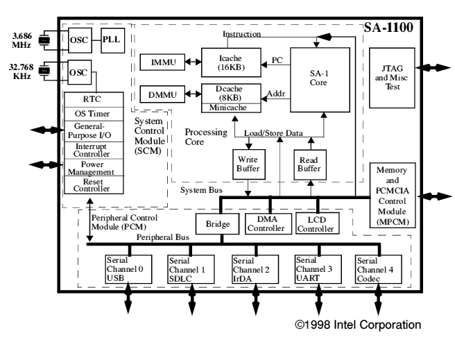
In September 1997, Digital announced the SA-1100 StrongARM chip. This includes the StrongARM SA-1 core, but adds on-chip memory interfaces, interrupt controllers, timers, serial ports and numerous other auxiliary and peripheral functions. In spite of the increased functionality, it still offers over 200 MIPS of processing power, and at a lower 0.2 watt power consumption. It is a fully static part (i.e. can be clocked down to 0 Hz) [10.5]. See figure 1.
Figure 1. SA-1100 Block Diagram The StrongARM SA-1100 implements most of a computer system on one chip! Capable of up to 200M instructions/s yet consuming only 200 mW, which reduces pro-rata with clock speed down to 0 Hz. The IHU-2 uses all the elements shown except RTC, DMA, LCD and Serial 0,1,2. All input/output is via the GPIO system at the left, and Memory Control on the right. Serial 3 is used for ground test at 115,200 baud; Serial 4 is used as a one-wire bus system. ©1998 Intel Corporation.
After consideration of various processors, the group decided to explore a design based on the SA-1100. Once that decision was taken, the memory size and technology were discussed.
For optimum operation of the StrongARM, a 32-bit wide memory system was indicated. Experience with RUDAK suggested that a large, protected memory space is counter-productive for power consumption. The MicroSat model of a smaller hardware-protected memory space for program execution, coupled with a software-protected larger memory space for data storage, was followed instead. The MicroSat computers are comparative power misers, and the design philosophy has proven to be scaleable with, for example, AO-27.
Using IPS, with roots in Forth, meant that a relatively small memory size would suffice. For example, AO-13 had 32K bytes of memory but never required more than half of this amount in spite of the complex operations it performed operating the spacecraft.
The memory size decided upon was 128K x 32-bit of hardware protected memory (EDAC) and 8 megabytes (2M x 32-bit) of software protected data storage.
Other early decisions included the use of a 400 bit/sec DPSK uplink and downlink for compatibility with the AMSAT community's existing command and telemetry hardware [9], CAN bus support, monitoring of the IHU on-board engineering beacon data stream, the use of programmable gate arrays to implement most of the hardware logic functions, and RAM-only memory system (no boot PROM).
The Design Review was held at the facilities of the Philipps University of Marburg, Germany, 1997 December 12-15. This was the only time the team was physically together. During these intense four days, the initial design was reviewed and substantially altered. It was at this meeting that the IQ modem was added, the single-wire expansion interface conceptually designed, and a FLASH memory chip included.
During the design process, the Internet proved to be invaluable in fetching the latest data sheets and specification of the parts to be used, and sorting through candidate parts in the search for the best available components.
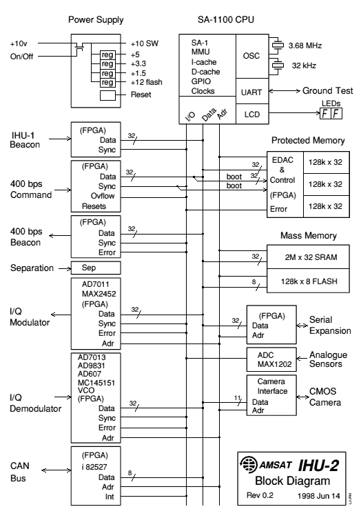
Figure 2. IHU-2 Block Diagram Almost all "glue" logic is subsumed into three QuickLogic 2005 gate arrays, saving space and substantially reducing development time. Complex signal processing ICs are used as indicated. Most blocks are managed via interrupts (15 sources) marked Sync, Error, Ovflow and Int. The IHU-2 consumes just 1.2 watts at 10 volts.
The Power Supply operates from the spacecraft +10V buses. After combining, the merged +10V is run through a FET power switch under direct control of the P3D IHU. When commanded on, independent switching power supplies provide the necessary +5V, +3.3V and +1.5V outputs needed by IHU-2. There is also a low duty-cycle +12V supply activated only when erasing and programming the FLASH memory.
The CPU consists of the SA-1100 chip and associated crystals. The part is so highly integrated that little else is needed.
The Protected Memory is composed of three (3) physical banks of 128K x 32-bit fast static RAM with error detection and correction (EDAC) logic implemented in a pair of QuickLogic field programmable gate arrays (FPGAs). A 2-out-of-3 majority vote system is employed, so that a bit may be corrupted in every memory bit location and the processor will still get accurate data. When an error is detected, the output from each memory bank is saved (96 bits total) as well as the address at which the error occurred. The processor may fetch this record for analysis or downlinking. In addition, the familiar 8-bit error counter is incremented, so that error rates as well as locations may be easily detected. Including correction delays, the memory system is designed for a nominal 70�ns access time.
Mass Memory consists of 8 megabytes of SRAM organized as 2M x 32-bit. This uses standard 4-megabit (512K x 8-bit) SRAM chips. Finally, there is a 128K x 8-bit Flash memory device using a 12-volt external power supply for erase and write. This type of memory was selected to avoid on-chip charge pumps, which are notoriously easily damaged by radiation.
Engineering Beacon data (for monitoring) passed from the IHU-1 is translated to 3.3V logic levels and passed into the FPGAs. Here, the sync vector is recognized, clock extracted, and differential decoding accomplished. The resulting data is presented to the CPU as 32-bit words, interrupt driven.
Uplink 400 bit/sec data is isolated by an op-amp, then sliced. The slicer output is fed into the FPGAs, where a digital phase-locked-loop (DPLL) recovers the clock. The recovered clock then operates an integrate-and-dump filter, and the output from this is passed back into the FPGAs for extraction of the data stream, differential decoding of the same, and block sync detection. A lock detector is also incorporated.
If the unit has just been powered up or commanded to "reset and load" then the recovered data is passed through the FPGAs directly to the protected memory array. After the uploading of the requisite number of words, the CPU is given access to the memory and begins executing instructions. If the CPU is already running, the FPGAs then assemble each 32-bit word and interrupt the CPU so that it can fetch the word and process it.
Downlink 400 bit/sec data is presented to the FPGAs as 32�bit words. The FPGAs convert the data to serial format, differentially encode it, multiply it by the 400 Hz clock, and shift the data out. This data is then changed to 10-volt logic levels for use by P3D. The FPGAs pace the data from the processor by means of interrupts. If data is not presented by the processor, the output of the uplink lock detector is used to change the downlink from a nominal 400 Hz square wave (unlocked) to a 200 Hz square wave (locked). This helps the command stations assure that the IHU-2 has acquired their command signal prior to commencement of uploading.
The CAN Interface uses the same Intel 82527 CAN controller and peripheral components that are used in RUDAK, the IHU and other CAN-equipped P3D systems.
A Ground Serial Port, modeled after the system developed for RUDAK, is provided for engineering unit development and testing. It is not powered or otherwise enabled in the flight unit. Likewise, a pair of HP 5082-7340 hex numeric LEDs are socketed on the board for debug purposes. These indicators are not fitted to the flight unit since they consume more power than the entire IHU-2, and no-one would see them anyway. They proved to be indispensable during testing.
The Camera Interface comprises 3V/5V CMOS translating buffers and a simple power switch. This allows the camera(s) to be switched on or off, and provides all needed signaling to control them and retrieve the image data.
An output from the Separation circuitry is scaled and fed to the processor so that it can determine if P3D is still attached to the launcher.
An IQ (In-phase and Quadrature) modem operates at the spacecraft IF of 11 MHz. The IQ Downlink uses an Analog Devices AD7011 IQ modulator operated in analog mode and fed a quadrature signal sample under interrupt control by the SA-1100. The SA-1100 parallel bus to AD7011 serial bus transformation and pacing logic is implemented in an FPGA. The output signal is filtered and scaled, then presented to a MAX2452 IQ modulator chip, driven by an external oscillator. The MAX2452 provides over 40 dB of carrier suppression, and the whole system draws only a few milliwatts. Output from the modulator is amplified by an AD8031 op-amp, filtered and matched to 50 ohms at an output level of -20 dBm. The downlink frequency is fixed.
The IQ Uplink signal is presented to a 50 ohm matched load, filtered, and amplified by an AD607 IQ receiver chip. The IQ output is filtered and matched to an AD7013 IQ demodulator, whose samples are de-serialized and synchronized, then presented to the SA-1100 as 32-bit words, interrupt driven. A DAC output from the AD7013 is used to provide gain control for the AD607 under control of the SA-1100. The chip lineup used is designed for low power portable devices such as cell-phones and draws little power.
The local oscillator for the uplink needs to be variable and controlled by the SA-1100. The means to do this in a low power fashion is to use an AD9831 direct digital synthesizer (DDS) chip driving the reference input of an MC145151-2 PLL. A VCO made from discrete components is used as the variable oscillator. The SA-1100 can command the DDS chip over a wide range of frequencies with very good resolution. In this way, the SA�1100 can compensate for doppler shift variations on the uplink as well as any other reasonable frequency drift, and close the loop for proper demodulation of the uplink signal using DSP techniques.
The IHU-2 includes an 8-channel, 12-bit A/D Converter. It is wired to monitor the +5, +3.3 and +1.5 volt power supplies as well as three temperature sensors (CPU, EDAC memory and unprotected memory). Additional inputs are provided to allow monitoring off-module parameters, none of which are currently defined for this mission.
Lastly, the one-wire Serial Expansion Interface is implemented in an FPGA with external level shifting. The external interface is designed as an open-collector of fairly low impedance to allow for a fairly fast transfer rate (4 µs/bit). Even with low impedance, because the duty cycle is very low, power dissipation is only a few milliwatts.
It is interesting to note that IHU-2 uses about half the number of ICs as the P3D IHU, has 130 times the memory capacity, operates 1,500 times faster, uses the same physical PCB size (200mm x 270mm), and consumes half the power - 1.5 watts!
The following table compares and contrasts the old IHU and new IHU-2 system:
                          IHU             IHU-2
  -------------------------------------------------------------
   CPU                  CDP1802         SA-1100-AA
   Buswidth             8 bits          32 bits
   Native MIPS          0.1             133 max
   Protected Mem        64K bytes       512K bytes
   EDAC *               1-bit           32-bit
   Unprotect Memory     none            8M bytes
   Nonvolatile Memory   none            128K bytes
   A/D                  8-bit           12-bit
   Expansion            Parallel        One-wire 32-bit serial
   Command Uplink       400 bps DPSK    400 bps DPSK
   Telemetry Downlink   400 bps DPSK    400 bps DPSK
   Other Up/Down        None            IQ Modem 20 Kbps max
   P3D CAN Bus          Yes             Yes
   Engineering Beacon   Generates       Generates or Monitors
                                           Engineering Beacon
   Size                 200mm x 270mm   200mm x 270mm
   Power                2-3 watts       1.5 watts
   Technology           Static CMOS     Static CMOS
   Rad Hard ICs         CPU, SRAM       None
  -------------------------------------------------------------

  * IHU EDAC can correct any single bit per 8-bit byte.
    IHU-2 EDAC can bit-wise correct a single bit error
    per bit location, or 32 bits per 32-bit word.
Electronic design matured over the period up to the end of January 1998. During this time it was reviewed and revised many times, until commitment to a PCB layout could be made (and time ran out).
The physical size of the PCB was fixed from the beginning. It would be a P3D standard 200mm by 270mm board. We did have an option to use multiple PCBs if needed but this would have added significantly to the cost. It would have also required wires between the PCBs. Wires are undesirable. Space on the board was at a premium from the beginning. So here is how it was used.
Power supplies: 20 percent. There are five different voltages used by various ICs in the design. Four of them required on-board power supplies. This does not count the RS-232 voltages generated by the ground support serial port (not used on the flight unit). There are also filters on the supplied 10V.
EDAC memory: 20 percent. The EDAC memory scheme used requires the actual memory to be three times as large as the processor sees. This is necessary to allow a two-of-three vote for each bit. This scheme results in a much faster memory system than the Hamming 12 to 8 EDAC system used on previous designs, in order to support the much faster processor.
Unprotected memory: 20 percent. There are eight megabytes of memory here. Any data placed here will have to be protected by software EDAC.
Voltage level converters/buffers: 20 percent. Generally speaking, the lower voltage an IC is designed to operate at, the less power it will consume (it's a square law too). And power is obviously very important in any satellite design. Unfortunately, not all functions are available in low voltage ICs. And the satellite interfaces between modules are typically 10v. Therefore quite a few voltage level converters are needed. This isn't as big a hit on space as you might think since these voltage level converters also function as buffers which, in most cases, would have been needed anyway.
Connectors: 10 percent. There are six connectors, digital and analog, along a 200mm edge. There are also two additional connectors along a 270mm edge which are not used on the flight unit (such as the ground support serial port).
Modems: 20 percent. This board wouldn't be much good without some way to communicate with it.
Miscellaneous: 20 percent. This includes things like telemetry gathering, CAN bus, and a cute little device called the SA-1100. The CPU is a 208 pin surface mount device with lead pitch of 0.5mm, more than five times closer together than a standard DIP IC.
Similarly the three FPGAs have 144 pins with leads on 0.5mm pitch. The FPGAs are mounted on daughter boards to facilitate logic analyzer connection and device removal. On the engineering units, daughter boards are socketed. Due to the tight board layout, it was essential to pre-define the three FPGA pinouts for PCB routing. The rich on-chip routing resources of the QuickLogic anti-fuse FPGAs allowed this pre-definition with no significant impact on performance. In the end, the FPGA utilisations were 99% of pins, 75% of logic and only 25% of routing resources consumed.
As usual, the total of used PCB space comes out at 130%. Nothing new here, most of our projects are like this. But somehow it always seems to fit.
The board is conservatively laid out using 10/9 rules (minimum trace width of 0.010 inches and minimum space between traces of 0.009 inches). The smallest drill size is 0.015 inches for vias. The board ended up being six layers (four signal, one ground and one power). The power plane was divided up to accommodate the various voltages used.
All of the ICs are surface mount devices. Most of the resistors, capacitors, diodes, and transistors are also surface mount. There are, however, quite a few thru-hole devices such as large capacitors, large diodes, inductors, voltage regulators and connectors. There are over 500 parts and almost 4000 soldered connections. The four PCBs (3 engineering, 1 flight) were entirely hand soldered.
A photograph of engineering model #3 is shown in figure 3, and a key to functional placements is figure 4.
 IHU-2 device statistics:

   Component   Surface-mount  Thru-hole
   --------------------------------------
   Capacitors      175          31
   Resistors       149           4
   Resistor packs   29           -
   ICs              77           -
   Transistors      13           3
   Diodes            6           7
   Inductors         4          13
   Misc              -           8
   --------------------------------------

   3769 solder joints
   519  electronic parts
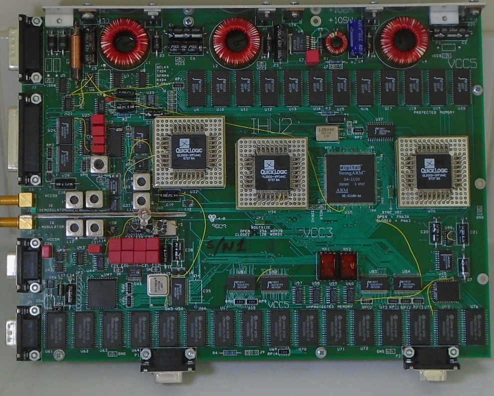
Figure 3. IHU-2 Photograph. Engineering model #1; six-layer board measures 270mm x 200mm. 341 surface mount resistors, capacitors, diodes, and transistors are underside. For flight, the board is surrounded by an aluminum frame/wall to which the connectors and PSU devices bolt. For thermal safety, CPU and both memory systems have heat shunts to the nearest wall. Lower connectors and LEDs are for test purposes only and do not fly, whilst the 3 FPGA daughter boards, presently socketed, are soldered down. The board is then conformally coated.
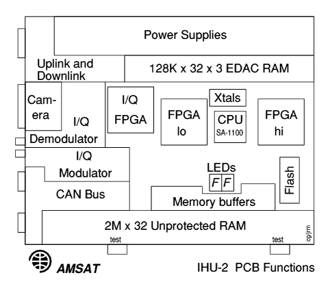
Figure 4. IHU-2 Functions Overlay This diagram complements the photograph. Connectors from top-left are Spacecraft Interface, Camera Interface, I/Q Demodulator IF I/P, I/Q Modulator IF O/P, CAN bus in, CAN bus out, I/O expansion (single wire), and Ground Test serial port (RS232).
Bringing up a new computer from scratch is a fascinating experience. It begins with the application of power and literally checking for smoke (done Orlando, 1998 Mar 11). This is then followed by voltage measurements throughout. Essential services such as clocks are checked, and gradually static reasonableness checks are made to all sub-systems.
Next, since this is a spacecraft computer, one first investigates the command input hardware (uplink) bootloading system. Once this works, simple test programs can be uploaded.
The very first program is typically minimal; drive the numeric LEDs at a rate of one count/second timed by delay loop. That's hardly a dozen instructions, but a successful outcome implies the satisfactory functioning of a considerable amount of circuitry, FPGA logic and CPU set-up. See figure 5. The IHU-2 ran this, its first program on 1998 Mar 27.
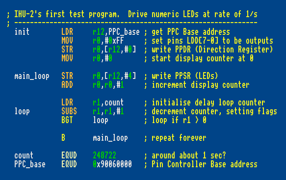
Figure 5. The first IHU-2 debug program. This one was written on Christmas Day 1997, 2-3 months before hardware existed. It worked first time. More demanding tests did not, and required regular software and hardware revision (coding and FPGAs), accomplished via the Internet. Later in the project (April 1998) the UK-AZ 8-hour time zone shift problem required a 5-day non-stop meeting in Tucson to complete the work efficiently.
The next program does something similar, but uses the external 20 ms interrupt to do the 1 second timing. This verifies that we can handle simple interrupts properly. Since there are 15 possible interrupt sources in the IHU-2, this is a useful exercise to get right.
The IHU-2 "talks" to the ground station via a beacon, so the next stage is a program that will drive the downlink system, also by interrupts. Its output is shown in figure 6. Data in the block is snatched from an SA-1100 3.68 MHz internal clock, and gives a clue to processor speed.
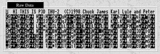
Figure 6. Downlink Screenshot The first telemetry downlink block from IHU-2, 1998 Mar 29. The data was time snatched from the SA-1100 internal 3.684 MHz timer, giving an indication of instruction speed (0.6 MIPS at that moment). Telemetry aficionados will notice the downlink CRC error. This was traced to having forgotten to enable byte accesses to memory. This simple oversight was the cause of early debug frustration, and shows why trivial clues cannot be ignored.
To conclude the I/O test phase, we check that there is input capability beyond the boot system. So the next test program is one that simply repeats any subsequent uplink straight back down on the beacon. This exercises two interrupt systems, and also requires circular buffer management to prevent input and output pointers from tripping over each other.
At this point we have verified that we have a computer system with the fundamentals, bootload, input and output functioning. In other words, a basically usable computer.
All subsequent work is checking that the CPU can communicate with the hardware sub-systems, and that those systems themselves work properly. In the order that we tested them; the unprotected 8 MB RAM, IHU-1 Engineering beacon monitor, I/Q modulator, I/Q demodulator, flash ROM read/write/erase, CAN bus, Camera interface, 1 wire serial interface, ground test UART. The memory EDAC system was checked by the simple expedient of omitting 1/3rd of the memory ICs (one bank) during PCB assembly. These ICs were installed later.
In all some 40 programs were needed. Most of the systems worked immediately. A few did not, particularly the specialised ICs used in the I/Q mod/demod circuits. However, manufacturers' support was willingly given, and all systems were eventually brought up to specification.
In addition to the test suite, two more important programs were written in this period. These were the Self-Checking Loader, and the AMSAT P3 Operating System IPS.
Acorn RISC Computers use ARM architecture processors, so the port of IPS to the IHU-2 was remarkably straightforward. It was simply stripped of all host computer specifics until just three "hooks" remained; 20ms interrupt, keyboard and screen. Conversion to the IHU-2 then only required substitution of these three elements by 20ms, uplink and downlink handlers of the IHU-2. When eventually uploaded to the IHU-2 (in late May '98), IPS came up working immediately.
Once an OS is running, programs can then be written in the native high-level language, IPS itself. Many IPS programs and library sub-routines exist already and run without problems.
The version ported to IHU-2 is called IPS-EM, and is 16-bit oriented, reflecting its pedigree. Much of an IPS implementation is written in IPS itself, and a substantial proportion of IPS-M high-level code is therefore identical to that of IPS-C/D (AO-13/P3D), both 16-bit environments.
The 32-bit version of IPS, called IPS-E, is presently being designed, and will be coded in the near future. It will be tested on an Acorn RISC Computer, and then ported to the IHU-2 in a manner similar to that described. IPS-EM is already blisteringly fast; IPS-E will improve on it by a factor of 2-3, as well as properly embracing the native ARM 32-bit architecture. This topic is dealt with by KM later in our paper.
The first processor using these principles, called ARM-1, was fabricated by VLSI in April 1985, and gave startling performance for the time, whilst using barely 25,000 transistors [1]. Building on that success, the ARM-2 was developed, and appeared first in a desktop computer in 1987, complete with a multi-tasking, mouse and window environment, drag n' drop, discless OS and much else. It was years ahead of its time, and whilst its prized successors continue in production, Acorn RISC Computers [10.2], along with many equally worthy platforms, have been eclipsed in popularity by global monopoly pressures in a largely naive marketplace.
ARM implementations continued to improve as microprocessor concepts and fabrication techniques advanced, finding wider application in high performance, low-power embedded systems. In 1990 ARM Ltd. was set up, with partners Apple and VLSI with the mission "To be the global volume RISC standard in the emerging markets where computing, communications and consumer electronics converge."
This has certainly been achieved. ARM based processors are in fabrication by a large number of partners, using ARM-6/7/8/9 and SA-1 macrocells. See [10.1] for a long list that includes VLSI, GPS, TI, DEC, Sharp and Samsung.
The embedded processor market is a quiet revolution; but the chances are that you used an ARM processor within the last hour; perhaps in your cell-phone; maybe at a "hole-in-the-wall" cash dispenser linked by ISDN half way across the planet. Who knows? Who cares!
ARM-60 processors are aboard TMSAT, TiungSAT and UoSAT-12 as part of their GPS experiments.
The SA-1100 part adopted for the IHU-2 is an embodiment of the ARM architecture undertaken by Digital Equipment Corporation over the period 1995-7. Costing around $30 in quantity, it offers some 200 MIPS of performance for a fraction of a watt of power. The SA-1100 process has recently been transferred to Intel Corporation.
   a) Fixed length instructions; 32-bits
   b) All instructions can be conditionally executed
   c) Lots of registers
   d) Data processing is register to register only
   e) 3 classes of instruction:
        Data processing    16 ADD SUB etc., 6 MULTs and a few processor
                              internal management
        Memory access       6 Load/store register(s) to/from memory
        Program flow        2 Jump, jump subroutine
Other features of the programmer's model, dealt with fully in [3], support a range of interrupts, traps and supervisor calls, all grouped under the general heading of Exceptions.
The ARM handles I/O as memory-mapped devices with interrupt support. That is, devices such as discs, parallel and serial ports, etc. appear as addressable locations within the ARM's memory map.
To support rapid context switching in multi-processing environments, the mapping between virtual addresses generated by the processor, and the physical addresses wired to the memory chips is definable in chunks from 1Mb to as small as 1Kb. ARM architecture handles this through a Memory Management Unit (MMU). Also supported are instruction and/or data caches. MMU and caches are on-chip in the SA-1100; the instruction pipeline is 5 tier. See [2] page 329.
Development tools (hardware and software) are available for many platforms, including the IBM-PC under W3.1, W95 and W-NT, various Unix systems, and Acorn RISC Computers. These tools use C, C++, JAVA and Assembler.
Programming in ARM assembler is best described as exquisite.
The ARM RISC Chip [1], also written by an ARM pioneer, takes a programmer's approach, and is weighted more toward the instruction set than the silicon. As does Furber, this book also contains fascinating historical material nowhere else recorded.
ARM Architecture Reference Manual [3] is the authoritative guide, and defines exactly what an ARM processor is. All ARM processors must conform to this text.
Data sheets for individual processors and core macrocells are available from their manufacturers, either on paper or via the Internet.
In contrast to the previous CCD sensors, these picture sensors can be read out like an EPROM. After applying an X and a Y address, the 8-bit value of the picture information is available for the selected pixel. The complicated timing and digitizing of picture data become totally unnecessary due to an on-chip flash Analog/Digital converter. There are no requirements regarding the read�out speed as with normal CCD camera chips. Pixels can be randomly read in any fashion, i.e. the same pixel can be read at high speed or sub windows of the pixel matrix can be accessed. The pixel address can be calculated "on the fly."
This is indeed a very important advantage compared to the standard CCD sensors with the more complex timing. Pixels can be read by an interleaving scheme, and thus the raw image resolution will�improve when more pixels are downloaded, etc. The maximum pixel rate of the CMOS Active Pixel Sensor is about 4 MHz. The user has full control over the number of pixels to read out and can exchange image resolution for frame rate.
In addition the CMOS APS exhibits superb picture characteristics, such as a very large logarithmic dynamic range of nearly 120 dB (6 light decades) in comparison to a normal CCD sensor with only 60 to 70 dB. The camera can see very bright and very dark parts in the same image.� The well-known "blooming" effects of overloaded CCD sensors also disappear. Pixels are non-integrating; after being activated they measure throughput, not volume. A saturated pixel will never overflow and influence a neighbour pixel. The dark limit is typical 1 lux (0.001 possible) compared to 0.1 lux (<0.0001 possible) of a normal CCD sensor.
Figure 7. CMOS Camera 512 x 512 imager shown in evaluation board configuration. From [10.3]
The camera used has a resolution of 512 x 512 pixels with an 8-bit resolution for the brightness information (black/white) [10.3]. The hardware effort is minimal, as is the interface to the IHU-2. The radiation hardness of CMOS APS sensors is exceptionally good at nearly 1 Mrad. Typical CCD sensors have a comparatively low radiation hardness of approximately 10 Krad.
The diameter of the earth is 16° at a distance of 47,000 km and 20° at a distance of 36,000 km. We decided to use a focal length of 17mm. With the optical sensitive area of 6.4mm x 6.4mm from our image sensor, this gives a Field of View (FOV) of about 21°. In comparison, the SCOPE cameras have a FOV of 16° for the Camera-A (narrow) and 32° for the Camera-B (wide). The precision optic for our camera is produced by Schneider Kreuznach. Because of the optical correction for the wavelength of 400 to 1000 nm, it gives very sharp images without focal difference for the whole visible spectra to the near infrared. Further, no additional IR blocking filter is needed, which will also improve the overall sensitivity. The APS sensor has a large spectral response from�400 to 1050 nm and fits perfectly with the above optics.
Originally it was planned to mount two of these cameras on the satellite. One camera on the upper side and the other on the lower side. The idea was to film and thus document the separation of P3D after launch. Comparably spectacular pictures have already been provided by TEAMSAT [10.4], launched with Ariane-502, which, as it turns out, employed the same camera technology.
Due to space limitations we decided to mount only a single camera on the upper side. Following separation it will still provide pictures of Earth. Later it can be used by IHU-2 as a navigation instrument in order to determine the spacecraft's orientation towards the Earth, and so enable attitude adjustment by the momentum wheels. It would be also possible to measure and track the daylight border line on the earth and re-orient the solar panels to the sun.
A subsequent job could be as star sensor for determining flight orientation, a task that the StrongARM SA-1100 could easily handle. The pictures from the camera will initially be stored in the 8 MB memory of the IHU-2. Without compression 32 pictures could be so stored. Appropriate JPEG compression would allow many more pictures, even a motion sequence to be stored. Pictures and motion sequences can be transmitted either through the IHU-2's own high speed DSP downlink or through the RUDAK experiment. In the second case, images will be transferred over the CAN network into the RUDAK Mailbox.
The CMOS APS camera is not intended to, nor can it, compete with the SCOPE experiment. It will be a technology demonstrator for future experiments.
An important limitation is the speed by which data can be transmitted between the satellite and the ground stations. The link performance, with distances up to 40,000 km, does not allow more than about 500 bit/s under worst-case conditions, and this only if better than the usual digital transmission techniques are used. For this reason, a format of 400 bit/s employing synchronous PSK was chosen [5].
Synchronous transmission formats are naturally block-oriented, so the adoption of PSK also suggested interacting with the computer in fixed length blocks - 512 byte blocks were chosen (with text this gives 8 lines with 64 characters).
In order to interact with the ground station computers, the same format was chosen. At the time this was a major departure from the "normal" way, because the typical computer of the time used character oriented teletype-like interfaces. Today it is normal to have a desktop with windows - but at the time the available video-units could barely support 16 lines by 64 characters.
Over the last 25 years the concept has proved its value, so there is no motivation to change it. It would be desirable to have higher interaction speeds with the spacecraft, but the link performance cannot be improved significantly. On the other hand the communication formats provide some margin by exploiting high-performance codes. This would in principle allow increasing the link-speed by a factor of 5���8. Presently we have provided a coded format for the uplink of the regular P3D IHU, not to increase speed, but to have error tolerance in case of interference. With the IHU�2, the hardware allows experimenting with speed-increasing codes.
Furthermore, it was required that at any time it would be possible to interact with the program on all levels. Thus the language handler was made interactive; just another task running along with the other tasks.
For the programming language itself, Forth was found to provide a good starting point, because this language is nearly syntax-free and naturally extendible. In fact the application-programs differ in no way from the original language-constructs. A major advantage was the fact that the system is extremely small compared to any other language handler.
But it also soon became clear that Forth was in many ways too limited for our purposes. In particular:
The interaction interface was designed from the start to use 512-byte blocks; thus many of the character-handling complications did not have to be addressed in the spacecraft. For the ground-station computers the same interface was adopted in various IPS-versions - early realizations of the windows concept.
The language itself was beta-tested in the University of Marburg keeping track of the typical errors during programming. This allowed identification of those areas which were particularly error-prone. As a result the language IPS was "cleaned up" and a couple of changes were implemented before freezing the design. Just to mention a few: name-redefinition was prohibited, names of objects can have any length using a hashing technique to encode them (all characters significant). Also a number of compiler checks were added to catch the more common blunders. For this reason four distinct classes of code were created.
For multi-tasking a three-level approach was chosen. Routines of moderate time sensitivity can be placed into a "chain" - all the operators in the chain are executed in a round-robin fashion. It is the programmer's responsibility to make sure that no task grabs the processor excessively. Some special routines have been provided to relinquish and recapture control when waiting for external events.
Tasks requiring quicker service, say every 20ms, have a way of interrupting the high-level address interpreter (the so called emulator pseudo-interrupt). Practically no overhead results from this approach when a stack-machine is interrupted. The interrupting routines can be either IPS or assembler. This approach guarantees the atomicity of IPS-instructions. The pseudo-interrupt turned out to be a very powerful concept and greatly helped to overcome the limitations resulting from the relatively small speed of the IHU.
For extremely time critical tasks, real interrupt and even DMA is included in this concept.
An unexpected side effect of the IPS stack�architecture is the property of the language to turn most programming mistakes into errors resulting in the wrong number of items on the stack. This is immediately visible and thus allows error detection very early on. Thus IPS-programs, once they run, probably have less hidden errors than programs written in syntax controlled languages. The net effect of this is that IPS has turned out to be a very useful tool to create ultra-reliable programs - for satellites definitely a welcome bonus.
Fortunately to redefine the word-structure to be 32-bit does not significantly impact the language itself. In fact most programs would run without any changes. Only programs which explicitly exploit the wrap-around properties of 16-bit words (like our angle representation used in the spacecraft) would need some modifications.
Basically the implementation also becomes simpler using the 32-bit words of the processor for the kernel-primitives. But there is a down-side; because now the addresses compiled by the system are 32 bit instead of 16 bit, the memory requirement about doubles. In practice, this is no problem, because during the last 25 years, computer memories have increased about 1000-fold. So a factor of two can easily be absorbed today - the system will be about 16 Kbyte large. Also this allows eliminating some of the specialised memory saving constructs of the old IPS (like 1 byte literals), making the system simpler.
The only remaining obstacle at this time (May '98) is that a different pseudo-code structure needs a new compiler. Previous versions of IPS have been compiled using a special meta-compiler (IPS-X) which creates the specific 16-bit pseudo code. Using this tool, the first 16-bit IPS for the IHU-2 (IPS-EM) was created [7].
For IPS-32, the meta-compiler must first be modified in order to compile the new target pseudo-code. All other tools have been built during the last 12 months on Acorn StrongARM RiscPCs, in particular an assembler for the StrongARM, written in IPS [8].
So it is probably only a matter of a fairly short time, until IPS-32 becomes available for both the IHU-2 and the RiscPC. Then the about 5000-times larger power of the StrongARM will be available from the very convenient IPS interface giving us unprecedented processing power to explore new software communication technologies both for space and for the ground-segment.
Chuck Green, N0ADI, did the PCB layout and constructed all engineering and flight units, as well as participated in the debugging process.
James Miller, G3RUH, ported the IPS operating system to the ARM and the IHU-2, wrote the vast amount of debugging code, assisted in the debug process in sunny Tucson and edited this manuscript.
Karl Meinzer, DJ4ZC, provided much of the stimulus for the project, embarked on the design of IPS-32, held out for the single-wire serial interface and IQ modem functions of the system, as well as hosted the design review less than two weeks before Christmas.
Peter Gülzow, DB2OS, initiated the discussions that launched the project, found the camera technology and researched and located much of the information needed in the early design discussions.
All the players participated in the intense design review meeting, evaluation and critiques of the evolving design.
Others who have made technical and logistic contributions include, with thanks, Werner Haas DJ5KQ (AMSAT-DL), Matjaz Vidmar S53MV (high speed data), Larry Brown NW7N (tantalum IC shields), Dick Jansson WD4FAB (heatsink metalwork), MMSI Tucson (test equipment), Stacey Mills W4SM (proof-reading) and our families (understanding).
AMSAT-DL agreed to fund the project, which almost immediately exceeded budget.
2. ARM System Architecture, S. Furber, Addison-Wesley 1996. ISBN 0-201-40352-8.
3. ARM Architecture Reference Manual, Prentice Hall 1996. ISBN 0-13-736299-4.
4. StrongARM SA-1100 Data Sheet V2.2, Digital Equipment Corporation 1997, V3.0 Intel Corporation 1998.
5. Die digitale Nachrichtentechnik der AMSAT-Phase-III-Satelliten, K. Meinzer, CQ-DL, 10/1978, pp. 447-453 [AMSAT Phase III Satellite Digital Communication Techniques.]
6. IPS - High Level Programming of Small Systems, K. Meinzer, 1978, 2nd Edition. Publ. by J. Miller 1997 ISBN 0-9530507-0-X. For availability see [10.13].
7. IPS-EM and IHU-2 Debug tools, continuously updated for IHU-2 group. James Miller.
8. ASSEMBLER FOR THE ARM, VERSION T.2 FOR IPS-M, Karl Meinzer, 2.11.1997, IHU-2 group document.
9. Phase 3 400 bps PSK Data Demodulator MK II. Oscar News 1992 Dec No.98 p39. PCB available; see [10.14].
10. Internet References
[JM: Since this article was written, the pace of technology was/is such that within 5 years, most of the links were broken. The products are not all obsolete; just the manufacturers' websites.]
[LJ: Intel yanked the StrongARM off the market to push us to Ball Grid Array X-Scale parts, thus making a lot of our effort on the IHU-2 become transient instead of foundational.]
10.1 ARM Ltd
10.2 Acorn RiscPC [ 2023 update; only second-hand machines nowadays! ]
10.3 CMOS Camera: http://www.vector-international.be/C-Cam/ccamindx.html
10.4 TEAMSAT photos: http://www.imec.be/fuga/cmos/vts.html
10.5 SA-1100: http://developer.intel.com/design/strong/
10.6 FPGAs: http://www.quicklogic.com/products/pasic2/ql2005.pdf
10.7 AD7013: http://www.analog.com/pdf/ad7013.pdf
10.8 AD607: http://www.analog.com/pdf/1824_0.pdf
10.9 AD9831: http://www.analog.com/pdf/ad9831.pdf
10.10 MC145151: http://mot2.indirect.com/books/dl110/pdf/mc145151-2rev2-1.pdf
10.11 Max2452: http://209.1.238.250/arpdf/1240.pdf
10.12 AD7011: http://www.analog.com/pdf/ad7011.pdf
10.13 IPS Book
10.14 P3 Demod PCB
Feedback on these pages to Webmaster. Feedback on the article should be sent to James Miller
Created: 1995 Feb 03 -- Last modified: 2023 Apr 17 [ URLs, IHU pic ]