The KD2BD Pacsat Modem

The KD2BD Pacsat Modem
This paper was originally published in the August 1994 issue of QEX: The ARRL Experimenter's Exchange. It was later published in the July/August 1995 issue of the AMSAT Journal, as well as the first edition of the ARRL's Packet: Speed, More Speed and Applications.
The KD2BD Pacsat Modem is a low cost, high performance 1200 bps BPSK modem designed to interface between a packet radio terminal node controller (TNC) and an amateur satellite ground station, and allows full-duplex access to the 1200 baud "Pacsat" constellation of amateur satellites.
Important features of this modem include:
The KD2BD Pacsat Modem was originally designed to interface with an MFJ 1270B terminal node controller (TNC-2 clone), and a Yaesu FT-726R multi-mode VHF/UHF communications transceiver. Suitable interfacing modifications should allow proper modem operation with other TNCs and ground station radio equipment. The specifics for doing so are left to the expertise of the reader.
Orbital Satellites Carrying Amateur Radio (OSCARs) have been a part of
amateur radio for over 30 years. With the growing popularity of terrestrial
packet radio communications on the amateur bands, recent OSCAR satellites
have been designed to make use of the AX.25 protocol in their communications
with ground stations. Some satellites, such as DOVE-OSCAR-17, use the
protocol for the transmission of telemetry information through beacon
transmitters, while others use the protocol to provide full duplex
communication links with the satellites' transponders. Amateur satellites
containing packet radio store-and-forward transponders are known as
"Pacsats".
The current roster of satellites making 1200 bps NRZI, HDLC, AX.25
protocol compatible packet radio transmissions on amateur frequencies
includes PACSAT-OSCAR-16, DOVE-OSCAR-17, WEBERSAT-OSCAR-18, LUSAT-OSCAR-19,
FUJI-OSCAR-20, ITAMSAT-OSCAR-26, and FUJI-OSCAR-29.
Of these satellites, only DOVE-OSCAR-17 uses audio frequency shift keying
(AFSK) modulation on a narrow-band FM carrier which is compatible with
existing terrestrial VHF-FM and UHF-FM packet radio communications. The
remaining satellites use binary phase shift keying (BPSK) modulation.
As popular and as widespread as the AFSK-FM method of transmission is
for 1200 baud packet radio communications, AFSK-FM and its popular
demodulation methods yield a level of performance that leaves a lot
to be desired. Steve Goode, K9NG, has shown through extensive testing
that a Tucson Amateur Packet Radio (TAPR) TNC-1 internal Bell 202 modem
required a signal level that produced at least 25 dB of FM receiver
quieting (25 dBQ) for high communications reliability. Since this is
a difficult signal level to achieve from micro satellites operating
on UHF frequencies with only several watts of transmitter power,
a more robust Binary Phase Shift Keying (BPSK) emission was selected
for use by 1200 bps Pacsat downlink transmitters.
Coupled with low binary data rates, Binary Phase Shift Keying has allowed
interplanetary space probes to transmit vast quantities of data to ground
stations on Earth from great distances with low transmitter power. BPSK
offers a 6 dB signal-to-noise ratio advantage over coherent CW (CCW)
modulation. CCW has long been considered to be the premium weak signal
communications mode available to amateurs.
BPSK is produced by modulating a carrier oscillator with binary modulating
information in a balanced modulator. The resulting BPSK emission can be
analyzed several ways, depending on whether the analysis is performed in
the time domain or the frequency domain. In the time domain, the BPSK
signal looks similar to the local carrier introduced to the modulator
except its phase shifts by 180 degree intervals with binary modulation.
In the frequency domain, BPSK looks similar to a double sideband suppressed
carrier AM signal centered about its local suppressed carrier frequency.
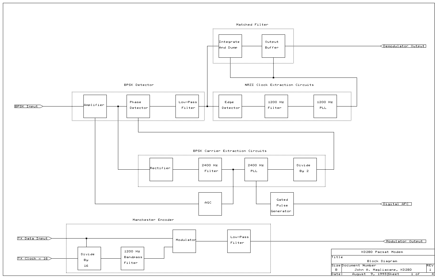
Figure One is a block diagram of the KD2BD Pacsat Modem. The demodulator
is designed to operate with an SSB receiver properly tuned to the frequency
of a BPSK transmitter. In essence, the SSB receiver merely acts as a
frequency converter, translating the RF BPSK signal captured by the ground
station antenna down to the audio frequency range where it can be easily
processed by the demodulator using audio circuitry.
The BPSK signal applied to the input of the modem branches in two
separate directions within the demodulator. One path extracts, processes,
and regenerates the BPSK carrier, while the second performs BPSK signal
detection and filtering.
BPSK signals in this modem design are demodulated synchronously, and
synchronous detectors require a reference carrier for phase determination.
Since the BPSK transmitter suppresses its carrier in its balanced modulator,
there is no clearly defined reference present in a BPSK signal. The
demodulator must therefore synthesize a BPSK reference carrier from
sideband components present in the composite BPSK signal. If viewed
in the time domain, the carrier of a signal whose phase shifts by
180 degree intervals may be extracted by taking the absolute value
of the BPSK waveform voltage and filtering the result. A full-wave
rectifier can be used to perform the absolute value function. The
rectification process yields a waveform of constant phase and frequency
twice that of the BPSK suppressed carrier. In the frequency domain,
the rectifier may be thought of as being a non-linear circuit that
mixes the upper and lower BPSK sidebands producing the algebraic sum
of those sidebands. Dividing the frequency of this product by two
produces a local carrier of constant phase whose frequency equals
that of the suppressed BPSK carrier.
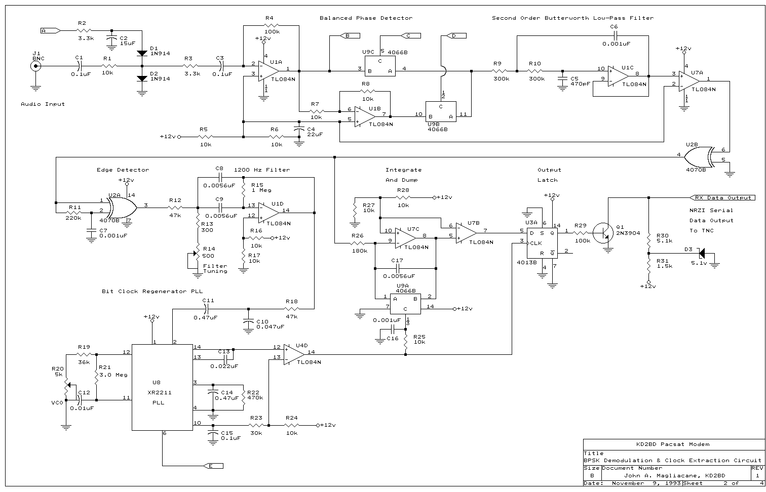
Referring to the schematic diagram of the KD2BD Pacsat Modem shown
in Figure Two, the received BPSK signal is first passed through a
current variable input attenuator. Resistor R1 acts as the series
element of an "L" attenuator. Diodes D1 and D2, that act as current
variable resistances form the shunt element. The AGC voltage that
drives the input attenuator is derived from the filtered BPSK carrier.
The level controlled BPSK signal is passed through input amplifier U1A,
after which it is split between the balanced phase detector and the carrier
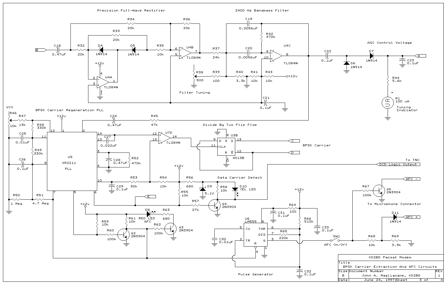
extraction circuits. The amplified BPSK signal is processed through a
precision full-wave rectifier circuit built around U4A and U4B, two sections
of a TL084N quad bi-fet operational amplifier. The output voltage of the
full-wave rectifier is the absolute value of the incoming BPSK signal.
If the downlink receiver is tuned such that the BPSK suppressed carrier
is at a frequency of 1200 Hz, then the output of the rectifier will
contain a strong product at twice this frequency, or 2400 Hz. Not only
does the rectifier mix the BPSK sidebands together, but it also mixes
noise components together creating even greater noise energy at the
rectifier output. In an effort to remove the undesired noise, the
rectifier output is filtered through a narrow bandwidth bandpass filter
built around op-amp U4C. This filter has a center frequency of 2400 Hz,
a bandwidth of 120 Hz and a Q of 20. The filtered carrier is further
processed through U5, an XR2211 Phase Locked Loop FSK Demodulator/Tone
decoder circuit with a loop bandwidth of 120 Hz. The XR2211 offers
outstanding frequency stability and provides several output signals
and other features used for receiver automatic frequency control (AFC)
and data carrier detection (DCD). The Phase Locked Loop regenerates
the 2400 Hz carrier, producing a noise-free waveform of constant amplitude
locked in frequency and in phase with that of the BPSK carrier.
The Phase Locked Loop's oscillator is extracted from pin 14, shaped to
a pulse waveform through op-amp U7D, and applied to U3B, a "D" flip flop
configured as a frequency divider. Toggling on the rising edge of each
input pulse, the flip flop divides the frequency of the PLL oscillator
by two, reproducing the 1200 Hz BPSK carrier with a 50% duty cycle as
required for proper operation of the phase detector.
The output of the 2400 Hz bandpass filter is also passed through a half-wave
peak voltage doubler and filter to generate a DC control voltage for the
automatic gain control system. Deriving the control voltage from the
filtered BPSK carrier results in an AGC that is virtually immune to noise
and interference that could otherwise affect the AGC and lead to demodulator
desense. The AGC control voltage also drives a front panel tuning and
signal strength meter.
The second path the received BPSK signal takes is the one that actually
extracts intelligence from the BPSK signal. A non-limiting, balanced
linear phase detector composed of operational amplifier U1B and CMOS
switches U9B and U9C is used to translate the BPSK input signal down
to baseband levels. The phase detector is driven by the locally
generated BPSK carrier supplied by U3B, and offers high local carrier
suppression and does not distort the wave shape of the BPSK signal.
It also helps to remove noise and other interference not in phase with
the desired BPSK signal.
In this design, linear AGC is used rather than hard limiting to maintain
a constant output voltage from the detector. As a result, strong input
noise does not corrupt weak BPSK signals since there is no limiter or
associated "capture effect" to suppress the weaker signal. Since the
phase detector switches at the zero crossing point of the sinusoidal
BPSK waveform, the detrimental effects of phase jitter and transmitted
phase noise are minimized.
The output of the phase detector is gently filtered through a second-order
Butterworth low-pass filter to remove higher order products generated by
the coherent demodulation process. The frequency response of the filter
loosely approximates that of the transmitted BPSK spectra, and its
smoothed output voltage is a function of how well the phase of the BPSK
signal correlates with that of the locally generated carrier. A perfect
correlation produces a maximum output voltage of one polarity, while a
correlation of opposite phase produces an output voltage of opposite
polarity.
The AX.25 packet radio communications protocol uses a data encoding
technique known as NRZI, Non Return to Zero Inverted. NRZI synchronous
data encoding packs both data and clock information into one binary
serial data stream. An NRZI receiver is edge triggered rather than
level triggered, and must therefore be sensitive to logic level
transitions and extract clock and data information from those transitions.
With NRZI, a '0' data bit is encoded as a bit level transition, while a
'1' is encoded as no transition. The AX.25 protocol uses a process
called zero insertion or "bit stuffing" that ensures that no more than
five '1's can occur sequentially except when flag bytes are transmitted.
Flags are used to identify the beginning and ending of each packet frame.
Zero insertion in combination with NRZI encoding guarantees that a logic
level transition occurs at least once every five bit periods. These frequent
level transitions are necessary to allow the modem and TNC to synchronize
with the transmitting TNC's clock.
In order to achieve the maximum demodulator performance possible, the
detected NRZI encoded serial data stream must be filtered to remove as
much noise as possible without introducing distortion that could lead
to data corruption. The detected baseband NRZI serial data stream present
after the Butterworth filter branches in two separate paths. One branch
extracts and regenerates the 1200 Hz bit clock from the NRZI encoded data
stream, while the other filters the NRZI data through an "integrate and
dump" processor that forms a matched output filter.
The unprocessed NRZI encoded serial data stream from the detector is
shaped to a square wave of constant amplitude through op-amp U7A and
further buffered through exclusive-OR gate U2B. The NRZI data is then
fed through an edge detector to extract clock pulses from the detected
waveform. The edge detector acts as a frequency doubler by multiplying
the NRZI serial data stream by itself delayed by one half of one bit period.
The RC network composed of R11 and C7 provides a one half-bit delay, while
exclusive-OR gate U2A performs the multiplication. The edge detector
produces an output pulse for every NRZI logic level transition received.
These pulses are in phase with the embedded NRZI clock signal and are
filtered by a 1200-Hz narrow bandpass filter, U1D. This filter receives
excitation from the edge detector and produces a damped sine wave by
virtue of its high 'Q' and the "flywheel effect". Its purpose is to
use stored energy to fill in the gaps during periods when NRZI bit
transitions do not occur and clock pulses cannot be recovered from the
edge detector. The damped sine wave output of this filter feeds U8,
an XR2211 PLL with a center frequency of 1200 Hz and a loop bandwidth
of 15 Hz. The phase locked loop follows the average phase and frequency
of the filtered NRZI clock pulses, and provides precise timing signals
required for operating the "integrate and dump" processor.
Maximum received signal-to-noise ratio (SNR) is achieved in a communications
system when the bandpass of a receiver exactly matches the bandwidth of the
transmitted signal. In order to achieve maximum signal-to-noise ratio, the
post detection filtering in this modem is performed with a filter matched
to the AX.25 binary data rate of 1200 bps. Unlike simple RC or LC filters,
the integrate and dump processor operates in the time domain and is
implemented with a resettable integrator and an output latch driven by
1200 Hz clock pulses recovered from the 1200 bps NRZI encoded data stream.
With a matched filter, the demodulator's output signal-to-noise ratio is
dependent not on the received signal-to-noise ratio, but rather on the
ratio of the signal energy to the power spectral density of the noise at
the filter's input. A matched filter allows the successful recovery of
weak signals buried deep in wideband noise, and offers the smallest error
probability that can be achieved and the best bit error rate performance
possible over an additive white Gaussian noise channel.
The unprocessed NRZI serial data stream from the phase detector is
integrated over each bit interval and the result is sampled by an output
latch. During each bit interval, random noise energy will accumulate no
charge across integration capacitor C17, while an input signal coherent
with the demodulator's internal BPSK reference carrier will accumulate a
charge either above or below this point depending on its phase. After
approximately 90 percent of the bit interval has passed, the voltage
integrated over this period is sampled and evaluated by comparing it
to a reference voltage equal to half the supply voltage. Operational
amplifier U7B operating as a voltage comparator performs this evaluation.
The result is sampled and latched by U3A, the CD4013B output buffer.
If the integrated .voltage is above the +1/2 Vcc reference, the output
buffer latches to a logic level '1'. If it is below this level, the
CD4013B buffer outputs a '0'.
Shortly after the output has latched, the integrator capacitor is
discharged and the process repeats for the next data bit. This time
averaging process of integrating, sampling, latching, and dumping produces
a well-filtered serial data stream re-timed to the recovered NRZI clock
signal. The output of matched filter is then converted to TTL levels of
0 and +5 volts through transistor Q1, and made available for processing
by the terminal node controller.
U5, the XR2211 phase locked loop used for BPSK carrier regeneration contains
an "in-phase" (I channel) detector to indicate whether or not the PLL is
locked in frequency and phase with its input signal. Since the PLL's input
in this case is a product of the BPSK carrier, the "in-phase" detector
indicates the presence or absence of a valid BPSK carrier on the modem's
input. U8, the XR2211 PLL used for bit clock regeneration contains a
similar "in-phase" detector. In this case, the detector indicates the
presence of valid 1200 bit per second clock pulses extracted from the
BPSK input signal. The active low, open collector outputs of both these
detectors are combined by connecting their outputs together. This combined
output is pulled to ground level when no carrier and no clock pulses are
detected, and to +5 volts when both a carrier and a 1200 bps clock stream
are present. It is buffered by Q4 to drive LED indicator D10 and is made
available to the TNC as a data carrier detect (DCD) control signal on
the output of the modem. The DCD line connects to the TNC serial I/O
circuits, and provides for on-the-air flow control and protocol timing.
The use of combined carrier and clock detection results in a DCD that
is very immune to noise and triggering from false signals.
Radio links between satellites and ground stations experience Doppler
effects due to satellite motion and the Earth's rotation. For an amateur
radio spacecraft in a low-Earth orbit of about 1000 km transmitting on
UHF, the magnitude of Doppler shift can be as much as 20 kHz, with a
maximum rate of change of 40 Hz per second at the time of closest approach
on an overhead pass. With the BPSK demodulator designed for a signal
properly tuned to within a few tens of Hertz, it is necessary to use an
automatic frequency control system to keep the downlink receiver properly
tuned to a BPSK transmission during a satellite pass.
An internal voltage comparator in U5 that is normally used for FSK decoder
applications of the XR2211 controls the logic of the Automatic Frequency
Control circuitry. The comparator compares the PLL error voltage to a
reference within the chip. If the error voltage exceeds limits dictated
by the PLL's loop bandwidth, it is an indication that the BPSK signal is
not properly in tune and the AFC circuitry is activated to affect a
correction. If the signal is tuned too high in frequency, the comparator
output voltage at pin 7 is pulled low, but only if a valid BPSK carrier
is detected on the input of the modem. If the voltage at pin 7 goes low,
it allows the LM555 gated oscillator to run stepping the downlink receiver
lower in frequency in compensation for Doppler shift. The receiver frequency
is controlled through a connection available on the transceiver's microphone
connector. Once the receiver frequency has been corrected, the comparator
output voltage at pin 7 returns high, disabling the LM555 oscillator,
keeping the receiver's frequency fixed until the next correction is
required.
Note that the AFC circuit employed in this modem can tune the receiver in
one direction only. Since the Doppler Effect causes the signal received
from a satellite in Earth orbit to drift lower in frequency during a pass
and never higher, it is only necessary to have the receiver tune lower in
frequency to compensate for the motion of the satellite. Front panel
switch SW1 enables the operator to disable the AFC feature of the modem
during manual receiver tuning.
Two digital AFC pulse polarities are produced by the modem. Output "AFC +"
produces a positive output voltage with respect to ground every time the
ground station receiver must be tuned. This polarity is consistent with
that required for Yaesu FT-726R transceiver tuning. Others require a
switch to ground, as provided by the "AFC -" output.
The ground station receiver must be capable of tuning in 20 Hz incremements
or less. If this is not possible, then it will be necessary to use an
analog AFC approach whereby the modem controls the voltage applied across
a varactor diode associated with the receiver's VFO.
Full access to the digital transponders on the Pacsat satellites requires
that ground stations use 1200 bps 3.5 kHz deviation Bi-Phase Manchester
encoded Frequency Shift Keying (FSK) for their uplink transmissions.
This is produced by feeding Manchester encoded binary data into the
microphone connector of a standard 2-meter narrow-band FM voice transmitter.
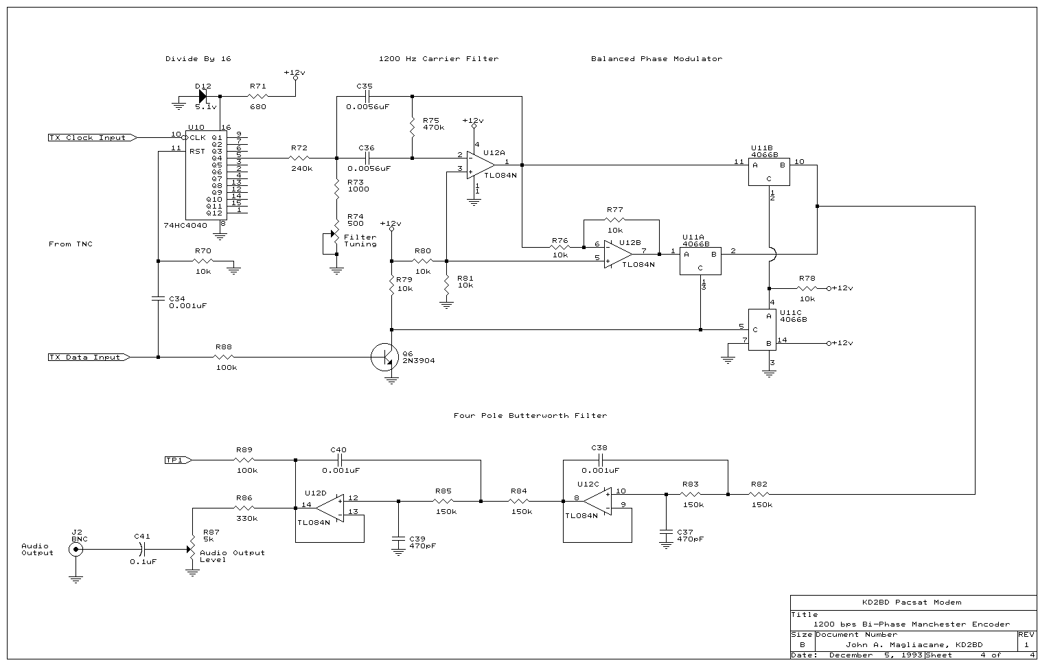
The KD2BD Pacsat Modem produces Manchester code by modulating the 1200 Hz
clock derived from the TNC with the 1200 bps transmit data in a balanced
phase modulator. The output is then filtered to produce a clean output
waveform that is low in harmonic distortion.
The TX clock available from the TNC modem disconnect header is at 16 times
the transmitted data rate, or 19,200 Hz for 1200 bit per second data.
The modulator divides this clock signal by 16 and combines it with the
transmit data in a phase modulator to produce a Manchester encoded data
stream. U10, a 74HC4040 ripple counter provides the necessary frequency
division. The divider is reset on the rising edge of the transmit data
waveform through R70 and C34 that form a differentiator network. This
synchronization keeps the divided clock waveform in proper phase with
the transmit data, and keeps the modulation switching transients at the
zero crossing points of the carrier waveform for minimum harmonic distortion.
The 1200 Hz square wave from the divider is then filtered through a 1200 Hz
bandpass filter designed around operational amplifier U12A to produce a
low-distortion sinusoidal waveform. The 1200 Hz carrier is modulated by
the transmit data from the TNC and the result is passed through a
fourth-order Butterworth low-pass filter. The purpose of the low-pass
filter is to reduce the sideband components of the output spectrum that
are a result of BPSK modulation. The Butterworth filter provides an almost
constant group delay across the entire modulator bandwidth, and results
in an output waveform having minimal zero crossing point dispersion and
phase jitter with modulation.
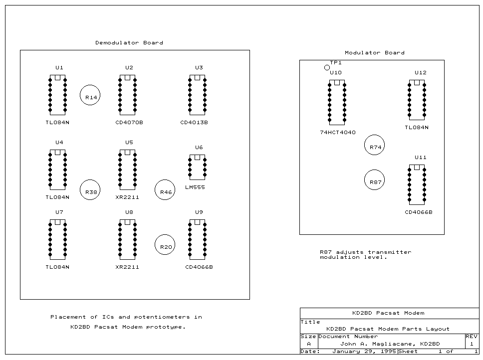
Initial alignment of the KD2BD Pacsat Modem requires the use of a high
impedance voltmeter and an oscilloscope. The modem should be connected
to the host TNC so an audio loop back test between modulator and demodulator
sections can be performed.
Set all potentiometers to their center positions. Configure the TNC for
a radio data rate of 1200 baud, and connect the TX Clock and ground from
the TNC to the modem and apply power to both the modem and the TNC.
Connect the oscilloscope to the modulator's high-level audio output
found at Test Point 1 (TP1) and verify the existence of a 1200 Hz
sinusoidal pattern on the oscilloscope. Adjust R74 (500 ohms) associated
with the bandpass filter in the modulator for maximum sine wave amplitude.
Connect TP1 to the audio input of the demodulator. Adjust the 2400 Hz
filter tuning adjustment potentiometer R38 (500 ohms) until the tuning
meter, M1, achieves maximum upscale deflection. With a DC voltmeter
connected between pins 10 and 11 of U5 (XR2211), adjust R46 (10k) until
the voltmeter reads zero volts. A 12 volt peak-to-peak, 1200 Hz square
wave should be present on pins 12 and 13 of U3B (CD4013B).
Attach the TX Data line from the TNC to the modem. The TNC produces
a series of AX.25 "flags" in its unconnected state that is sufficient
for testing the clock extraction and regeneration circuitry of the modem.
Using the oscilloscope, verify the presence of a pulse train on pin 3 of
U2A (CD4070B). A damped sine wave should be present on U1D pin 14 (TL084N).
Adjust potentiometer R14 (500 ohms) for maximum sine wave amplitude as
seen on the oscilloscope. With a DC voltmeter connected between pins
10 and 11 of U5 (XR2211), adjust potentiometer R20 (5k) for a reading of
zero volts. At this point, the DCD indicator should be on and the AFC
indicator should be off. Trigger the oscilloscope's internal horizontal
sweep to the recovered clock pulses present on pin 14 of U4D (TL084N).
Monitor the waveform present on pin 8 of U7C (TL084N) and re-adjust
potentiometer R14 for the tallest and cleanest pattern of right triangles
seen on the oscilloscope. An "eye diagram" can be viewed by monitoring
the waveform on pin 8 of U1C (TL084N) while triggering on U4D pin 14.
At this point, the modem is fully aligned and is ready for operation.
You should be able to establish a packet connection with yourself at
the keyboard as a verification that both modulator and demodulator
sections of the modem are functioning properly.
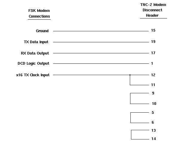
The KD2BD Pacsat Modem requires several connections to the host TNC as
well as the ground station radio equipment. Connections to the TNC's
internal modem must first be broken so the following connections to the
pacsat modem can be made. Received data from the modem is directed to
the TNC via the modem disconnect header available on many terminal node
controllers. RX Data from the modem is connected to pin 17. DCD logic
from the modem connects to pin 1. Transmit data from the TNC connects
to the modem via pin 19, and the transmitter clock (x16) from the TNC
attaches to the modem through pin 12. Consult your owner's manual for
the specifics of connecting an external modem to your TNC.
Connections must also be made so the TNC can key the uplink transmitter.
Modulator audio from the modem connects to the microphone connector of
the uplink transmitter. AFC pulses from the modem trigger the downlink
receiver tuning, and simulate a user pressing the microphone's "down"
frequency button. Audio from the receiver connects to the modem's audio
input. As with the TNC, consult the owner's manuals of your ground
station radio equipment before making any connections to the modem.
Once connections between the modem, TNC, and ground station radio equipment
have been made, on-the-air operation can begin. With the modem's AFC switch
in the off position and the receiver in the USB mode, tune in a satellite
transmitting 1200 bps BPSK. Slowly tune across the BPSK signal until the
tuning meter achieves maximum upscale deflection. The tuning meter will
indicate several peaks when tuning across a BPSK signal. Correct tuning
is achieved when the receiver is tuned to the center of the highest
peak. When properly done, the yellow DCD indicator should be on and
you should be able to copy packets from the satellite on your computer
terminal. Switch the AFC on to activate the modem's automatic frequency
control. As the red AFC indicator comes on, the receiver should tune
lower in frequency in compensation for Doppler shift. The KD2BD Pacsat
Modem is very sensitive and will successfully track BPSK signals barely
audible through the background noise. At this point, the yellow DCD
indicator should be on and you should be able to copy packets from the
satellite on your computer terminal.
Potentiometer R87 (5000 ohms) should be adjusted for a modem output
audio level that produces approximately 3.5 kHz peak carrier deviation
of the uplink transmitter. Greater levels of modulation will cause the
uplink signal to deviate out of the 15 kHz-wide Pacsat uplink receiver
passband.
To communicate with the satellite, adjust your uplink transmitter to one
of the transponder uplink frequencies and set your TNC for full-duplex
communications (FULLDUP ON). Sending a connect request should result
in a connection to the satellite. The actual procedure for communicating
with the satellite's mailbox will depend on the Pacsat being accessed and
the ground station terminal software required for access. FO-20 operates
in a fashion similar to a typical terrestrial packet bulletin board running
PRMBS software and can be accessed without the need of Pacsat terminal
software, such a "PB".
Reception of WEBERSAT-OSCAR-18's CCD Earth images does not require the
use of an uplink transmitter or the modulator portion of this modem, but
does require the use of Microsat ground station software and WEBERSAT
image display software. The Pacsat Beginner's Guide, containing Microsat
Ground Station software, and "Weberware" for use with OSCAR-18 are available
from:
The KD2BD Pacsat Modem was designed independently without the luxury of
having seen other previously published Pacsat modem designs. It is the
result of countless hours of research, experimentation, and testing. Many
different modem configurations were attempted over the design period with
the one described here providing the best overall performance. One of
the major design goals of this modem was to produce a modem capable of
demodulating very weak signals. The performance demonstrated by this
modem shows these design goals have clearly been met.
So whether your interests are in viewing the world through the eyes of
WEBERSAT, setting up an electronic mail gateway through PACSAT, or just
reading the latest issue of SpaceNews on OSCAR-20, you will find
the KD2BD Pacsat Modem is a valuable accessory for your TNC and a welcomed
addition to your OSCAR satellite ground station.
See you on the birds!
Goode, Steve, "BER Performance of TAPR TNC Modem", QEX, August 1983,
pp 3-4
Jordan, Edward C. Reference Data for Engineers: Radio, Electronics,
Computer and Communications, 7th Edition, 1986, pp 24-5 to 24-6, 24-12
to 24-15
Schwartz, Mischa, Information, Transmission, Modulation, and Noise, 1970,
pp 431
Carter, Max, "Super Narrow Techniques Equalize Power Inequity on 1750 Meters",
Communications Quarterly, November 1990, pp 99-113
Miller, James, "Data Decoder for UoSAT", Wireless World, May 1983,
pp 28-33
The Pacsats
Binary Phase Shift Keying
BPSK Signal Processing
BPSK Carrier Recovery
BPSK Signal Detection
NRZI Data Encoding
Post Detection Filtering
Bit Clock Regeneration
Integrate And Dump
Handshaking Controls
Automatic Frequency Control
Data Modulation
Alignment And Testing
Modem Operation
	AMSAT-NA
	850 Sligo Avenue
	Silver Spring, Maryland  20910
	USA
Summary
Bibliography
Schematic Diagrams